Design Porting
Anolog Layout
Ciris Semi supports customers in Layout activities related to Analog Design, Full Custom Design and Standard Cell Design. Our layout expertise from 180nm to 22nm
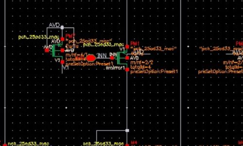
Design porting from different technology node & Foundries
If customer is looking for Migrating designs as per Market requirement, Performance, Cost and Flexibility in choice of a foundry, Ciris Semi support it.
First Ciris Semi can do the feasibility analysis and submit reports on advantages/disadvantages and design constraints wrt a baseline and a target node.
Engagement Model
Ciris Semi has a flexible and mutually sustain model as per customer requirement.